Next: Feature Preservation using Resistive Up: Resistive Fuse Networks Previous: Resistive Fuse Networks Contents
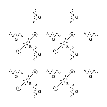
In a resistive grid, each input voltage source is connected directly to the
output node by a resistor of resistance ![]() . Each output node is also
connected to each of its neighbours by a conductance
. Each output node is also
connected to each of its neighbours by a conductance ![]() . A
section of resistive grid is shown in Figure 3.1.
. A
section of resistive grid is shown in Figure 3.1.
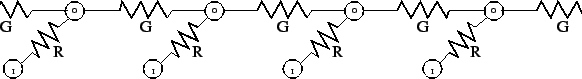
The operation of a resistive grid is most easily described in terms of a one
dimensional resistive grid, as shown in Figure 3.2.
A voltage difference between each pair of nodes will create
a current between them through the conductance ![]() ,
which will tend to equalise their voltages. As
shown in Figure 5.1, if there is a spike in the input,
neighbourhood action will tend to reduce the value of the spike. In so
doing, neighbourhood
voltages will be raised. However, their neighbours will drag them
down as well. So the spike will be affected, and affect, not only its
immediate neighbours, but every pixel in the image. In a one dimensional
network, the effect drops off as an exponential function of
distance from the spike. If each voltage source is connected to the node by
a conductance
,
which will tend to equalise their voltages. As
shown in Figure 5.1, if there is a spike in the input,
neighbourhood action will tend to reduce the value of the spike. In so
doing, neighbourhood
voltages will be raised. However, their neighbours will drag them
down as well. So the spike will be affected, and affect, not only its
immediate neighbours, but every pixel in the image. In a one dimensional
network, the effect drops off as an exponential function of
distance from the spike. If each voltage source is connected to the node by
a conductance ![]() , and the resistance between nodes is
, and the resistance between nodes is ![]() , then the voltage
at each node as a function of distance
, then the voltage
at each node as a function of distance ![]() from the source of voltage
from the source of voltage ![]() is given by [11]:
is given by [11]:
where ![]() is called the characteristic length, in number of nodes, and is
given by
is called the characteristic length, in number of nodes, and is
given by
In a two dimensional network, the effect is given by a modified Bessel function rather than an exponential:
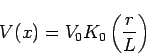
where
The result is much the same though. The effect of a spike in the input is felt as a rapidly decreasing function of distance over the entire network. This is similar to the computer-based equivalent algorithms, which use a bell shaped impulse response filter convolved with the input image. Although the digital filters are usually limited in size, distant pixels in a resistive grid have only a vestigial impact, so the effect is approximately the same.
The dependence on ![]() means that the width of the area over which a
pixel is smoothed depends critically on the resistance of the network.
means that the width of the area over which a
pixel is smoothed depends critically on the resistance of the network. ![]() is usually fixed by the detector design process, but if
is usually fixed by the detector design process, but if ![]() can be
independently set as a global parameter, then the operation of the circuit
can be finely adjusted. Adjustability of the resistance is one of the
motivating factors in the choice of practical devices discussed later.
can be
independently set as a global parameter, then the operation of the circuit
can be finely adjusted. Adjustability of the resistance is one of the
motivating factors in the choice of practical devices discussed later.
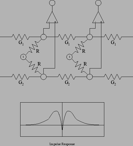
A simple resistive grid produces the effect of convolving the input image with an exponentially decreasing impulse response. It is possible to achieve this effect with differently shaped filters, by using multiple resistive grids in parallel, and then taking the weighted sum of the output nodes of these resistive grids as the output voltage, as shown in Figure 3.3. This strategy was used in a simple form by Mead and Mahowald to achieve an approximation to a difference of gaussian filter used by Marr and Hildreth for their silicon retina [12]. More complicated networks are usually too complicated to implement in practice.
Another way of looking at a resistive grid is to consider it as an adaptive system with two counterbalancing forces. The source resistor can be considered as trying to bring the output nodes close to the source voltage. The interconnect resistors are trying to make output nodes as close as possible to each other.